Author: National Renewable Energy Laboratory[1]
The term generic is used to describe a model that is not specific to any manufacturer, which means that a dynamic model should be able to represent PV inverters from different manufacturers and not be specific to only one manufacturer. Different editions of PV inverters from the same manufacturer may implement similar control strategies but different ranges of settings. For example, various regional or market segments may have different grid codes, and a PV inverter may be set to accommodate local grid codes. The input parameters of the dynamic model to represent the PV plant at this location must be adapted accordingly. The dynamic model is also an open source; thus, it is easy to modify. Only the original file will be kept unchanged. The model also needs to be flexible so that changes can be made and/or added to the control block diagram to suit the specific design of a PV inverter or a specific PV plant. Also, this model is based on three phases; thus, the three phases—a, b, and c—are represented, instead of positive sequences only. This means that all the symmetrical components—positive sequence, negative sequence, and zero sequence—can be represented. This is important for a PV inverter, because many PV inverters are single phase, and many PV inverters are installed in the distribution network, which is susceptible to unbalanced conditions (from the network or voltages). The completed PV generation dynamic model developed in this subtask is built on the PSCAD platform. The PV industry lacks such a model, and this project proposed to fill that gap down to the switch details via PSCAD. PSCAD allows for the analysis of unbalanced faults, such as single-line-to-ground (SLG) or line-to-line-to-ground (LLG), a key characteristic distinguishing PSCAD models from other dynamic models that focus on positive sequence behavior (e.g., Positive Sequence Load Flow (PSLF) and Power System Simulation for Engineering (PSSE)). This program is intended as a cycle-by-cycle model of PV inverters, and it is built with detailed circuitry of the power converter (including the power semiconductor switches); thus, a detailed analysis of a PV inverter can be accomplished. For example, we can observe the dynamic of the voltage on the direct-current (DC) bus during the transmission faults, or we can observe the dynamic of the output currents and powers when one of the power semiconductor switches is damaged or misfired. The model is also intended to include the collector system of the PV plants and other plant-level controllers. The control architecture is based on the one developed by the Renewable Energy Modeling Task Force of the Western Electricity Coordinating Council (WECC). There are three major blocks: the (1) renewable energy plant controller (REPC), (2) renewable energy electrical controller (REEC), and (3) renewable energy generator controller (REGC).
The process of PV generation from the PV cell to the power converter, which includes the maximum power point tracker, is described in the PSCAD Modules Representing PV Generator article. Here, the different types of power converters, the control implementation, and the dynamic model validation is presented.
Contents
- 1 Basic Three-Phase PV Inverter
- 2 Controlling the Grid-Side Inverter and Power Plant
- 2.1 Device Level
- 2.2 Generator Level
- 2.3 Plant Level
- 3 PV Dynamic Model Validation
- 4 References
Basic Three-Phase PV Inverter
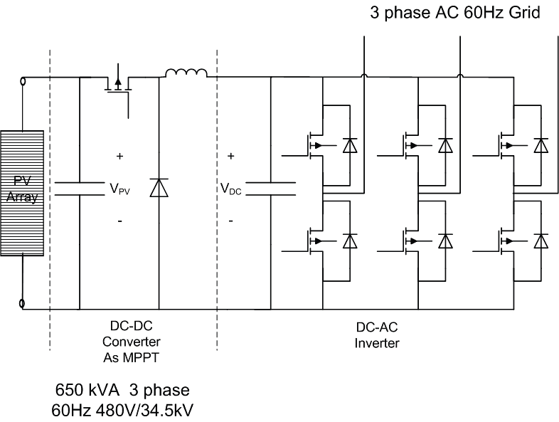
A three-phase PV inverter is usually designed for a three-phase system with a large rating (10 kW–2 MW and above). Most PV inverters are current controlled. To understand a basic PV inverter, it is important to understand the module and PV inverter hardware. In general, a PV inverter consists of a DC bus and three pairs of power semiconductors, also called power electronic switches or power switches. The most common power switches presently used are insulated-gate bipolar transistors (IGBT). An IGBT can be turned on and off very fast within microseconds (thus, the loss from power switching is low), and it has a low conduction loss.
Basic Control of Real and Reactive Power in a Two-Bus Power System
In this section, we use a two-bus system to illustrate real and reactive power for conventional generation and generation based on power converter based generation. We assume that the generator, Vpv (Bus 1), is connected to an infinite bus, Vs (Bus 2). In a conventional power plant with a synchronous generator, the following quantities are usually used to control the output of the generator:
- The voltage magnitude is used to control the reactive power (or reactive current component, Iq by controlling the excitation winding, thus increasing the voltage of Vpv.
- The mechanical power is used to control the phase angle of the output voltage of the synchronous generator. The power angle, δ, of the output voltage mostly corresponds to the real current component, Ip, of the output current, Is, of the voltage source.
A similar method can be used for a PV inverter, except we attempt to control the current directly.
Conventional Power System
Reactive Power Control

To understand a PV inverter and to simplify the analysis, let us consider an average model. Because the relationship of the reactive power to the terminal voltage is very tight, either the reactive power control or the voltage control is generally used. The phasor diagram concept is very useful to visualize the real power, reactive power, voltage, and current. It is also timely, as the synchrophasor measurements to monitor these quantities are available and have been installed massively in the modern power system network.
To describe the relationship between the reactive power flow and the voltage level, refer to the phasor diagram on the right. It is assumed that the PV inverter (terminal voltage, Vpv) is connected to an infinite bus, Vs, through a reactance, Xs. The PV inverter (Vpv) generates an output current, Is. The equation describing the relationship of the voltage at the two buses and the corresponding voltage drop across the reactance, Xs, can be written as follows
\(V_{pv}=V_{s}+jX_{s}I_{s}\)The reactive power losses (Is2Xs) in the transmission line can be supplied from Bus 1 (Vpv) or Bus 2 (Vs), or they can be shared by both sides. Parallel compensation (e.g., capacitor banks) can be implemented on both sides. Reactive compensation can be implemented by controlling the generator itself (internal control), or it can be provided externally, such as from adjustable capacitor banks, synchronous condensers, and static power compensation (a static VAR compensator, SVC; or static compensation, STATCOM).
Consider the PVP simplified equivalent circuit, in which all the reactive power spent in the reactance, Xs, is supplied by Bus 1. As shown, the voltage Vpv > Vs, to make it possible for the reactive power to flow from Bus 1 to Bus 2. Similarly, all the reactive power spent in the reactance, Xs, is supplied by Bus 2. In this case, the relationship between the two voltages is Vpv < Vs. Now consider another case, in which the voltages at Bus 1 and Bus 2 are maintained constant, and there is equal magnitude at 1.05 p.u. The reactive power is supplied equally by both Bus 1 and Bus 2. The voltage Vpv = Vs requires that the source of the reactive power comes from both sides. Thus, the larger the contribution of the reactive power, the higher the voltage of the source of the reactive power.
Real Power Control

The equation describing the relationship of the voltage at the two buses to the corresponding voltage drop across the reactance, Xs, can be written as follows
Real power output can be increased in many ways. For example, increasing the real power output while maintaining equal voltage (Vpv = Vs) can be illustrated by the changes shown in the phasor diagrams on the right. As mentioned above, in this equal-voltage condition both sides share the reactive power loss in the line reactance, Xs, equally. As the current, Is, increases, the power angle, δe, also increases while equal voltage is maintained (Vpv = Vs).
Power-Converter-Based Power System
Reactive Power Control

Figure on the right illustrates the power converter based power system and its corresponding phasor diagram. The PV generator is connected to a grid through a reactance, Xs. The current, Is, is decoupled into real and reactive components (Ip1 and Iq1). Assuming that the grid is an infinite bus, Vs is constant. The impact of reactive power’s contribution on voltage regulation can be illustrated by the appropriate phasor diagrams. The phasor current, Is, is divided into the real current, Ip, (in phase with the voltage Vpv) and reactive current, Iq, (in quadrature with respect to the voltage, Vpv) components.
The voltage equation is rewritten as
\(V_{pv}=V_{s}+jX_{s} \left (I_{p}+I_{q} \right )\)The real current component, Ip, is proportional to the real power generated, and the reactive current, Iq, is proportional to the reactive power generated. Doubling the reactive current, Iq, will double the voltage drop, IqXs, and directly increase the terminal voltage, Vpv, by an additional IqXs. Thus, to increase reactive current, we need to increase the voltage, Vpv. The larger the value of Xs, the higher the voltage, Vpv, will increase as the same amount of the Iq current is increased. As can be expected, increasing the reactive component of the current, Iq, will directly impact the terminal voltage magnitude, Vpv, and increasing the real current component, Ip, will more directly impact the power angle, δ, between Vpv and Vs.
In PV generation, two limits must be observed:
- The total resultant current, Is, is limited by the maximum current-carrying capability of the power converter (Imax). Thus, the power converter can increase its real or reactive current components (or both) only to a certain level, until the resultant current reaches its maximum (Is = Imax – current-carrying capability of the IGBT switches). At that point, the overcurrent protection will prevent the PV inverter from delivering more current.
- The maximum terminal voltage, Vpv, must be limited to the maximum voltage of the power converter. Thus, the power converter can increase its reactive current component, Iq, only so much, until the terminal voltage reaches its upper limit. At that point, the overvoltage protection will prevent the PV inverter unit from delivering more reactive current to the grid.
Real Power Control

The phasor diagram to demonstrate real and reactive power control in a PV inverter shows the size of the real current component increased to Ip2, while the size of the reactive current component, Iq1, is maintained. The additional voltage drop, jXsIp2, is shown to increase by the same proportion. This affects the increase in the angle between Vpv1 and Vs. Because the size of the infinite bus, Vs, is constant, the increase in Ip increases the voltage drop, but it decreases the voltage, Vpv2. The size of the reactive current component stays the same, and the resulting voltage drop, jXsIq2, also stays the same size. Note that the voltage, Vpv, decreases from Vpv1 to Vpv2. To return Vpv2 to the same level as Vpv1, the reactive current component, Iq, is increased to Iq2. This indicates the size of the voltage, Vpv1, and the size of the current, Ip2. The increase in the output power is proportional to the change from Ip1 to Ip2, and the reactive current contribution to cover Is2Xs loss are equally distributed between Vpv and Vs.
Current-Source Inverter (CSI)—Average Model





Presently, most power converters are current-source inverters (CSIs). In the power drives, the current-control converter gives a very fast response to the torque required. In a grid-connected power converter, the current-control capability can give a quick response to the real and reactive power demand.
We consider an average model one of an ideal power converter that can generate a sinusoidal current (with no harmonics). Thus, we simulate a PV inverter as a sinusoidal-current source. The output current is synthesized to give a sinusoidal output current that has a controllable magnitude and phase angle. In a PV inverter, it is common to control the real (Ip) and reactive (Iq) components of the output currents.
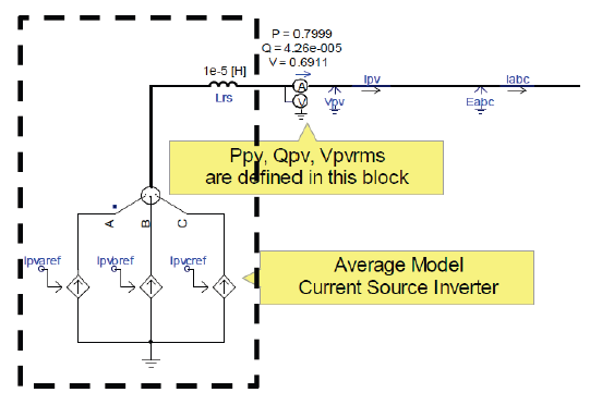
The one-line diagram of an average model of a CSI synthesizing a PV inverter shows a three-phase PV inverter (an ideal model of a three-phase current source) connected to the grid. The DC-AC (alternating current) inverter has two major functions: (1) to control the real power output of the PV strings and (2) to control the reactive power output. In actual PV generation, the control of the real power is very simply implemented by maintaining a constant DC bus voltage while the controlling the DC-DC converter to maximize the output power of the PV module.
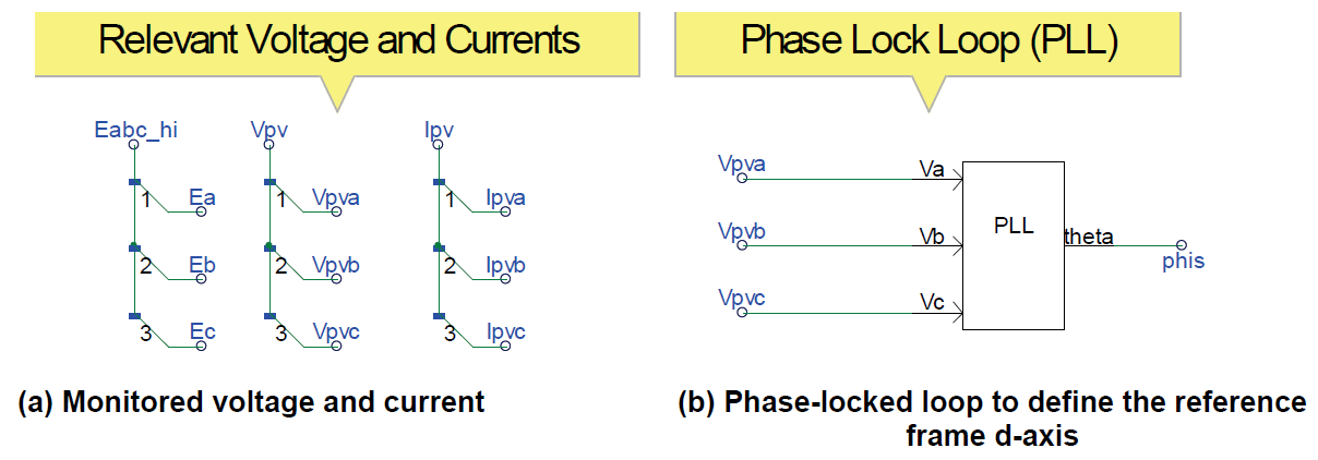
The CSI is the block inside the rectangle marked by the dashed black lines. The first thing to consider when controlling a CSI is to find the reference frame at the point of measurement to which it is connected. In this case, the reference is the terminal voltage of the PV inverter. The voltage sensor is placed at node Vpv, as shown. Similarly, the real (Ppv) and reactive power (Qpv) sensors are inside the multi-meter at the Vpv node.
Figure on the right shows a simplified equivalent circuit of the current source producing the output current, Is. Using the d-q axis synchronized to the phasor voltage, Vpv, we can decouple the current, Is, into its d-axis component (real current; Id = Ip component) and the q-axis, the reactive current component, Iq. The real current component, Ip, is used to control the output real power of the PV inverter. The control of the reactive current component, Iq, is used to control the reactive power output of the PV inverter. PV inverter generates reactive power into a regular (non-infinite bus) grid. The terminal voltage increases as the reactive power output of the PV inverter increases. Consequently, controlling the reactive current component, Iq, can be used to control the terminal voltage and vice versa.
The equation for the current can be expressed in a complex number
\(V_{pv}=V_{pv}∠0^o\) \(I_{s}=I_{s}∠-\Phi_{ο}\)Based on the arrow direction, by definition (generator convention), the apparent power generated by the PV inverter can be written as:
\(S_{pv}=V_{pv}⋅I_{s}^{*}=P+jQ\) \(P=V_{pv}⋅I_{s}⋅cos \left (\Phi_{ο} \right )\) \(Q=V_{pv}⋅I_{s}⋅sin \left ( \Phi_{ο} \right )\)The current conjugate of the output current is expressed as Is*. Thus, both the real power and the reactive power have positive values (generated from the PV inverter).
The phase-locked loop is the synchronizer that will latch the reference frame to the synchronous reference frame attached to the voltage phasor, Vpv, at the terminal of the PV inverter.
Note that after we found the reference frame of the terminal voltage, the real current component (Ip) and the reactive current component (Iq) can be oriented with respect to the “direct axis,” which has the same phase angle of the the terminal voltage, Vpv. Note that the subscript “p” indicates the real power component, and “q” indicates the reactive power component. The real power component, Ip, is represented by the “direct” axis component (in phase with the synchronous reference frame, “d”); thus, it is sometimes used to indicate Ip = Id; whereas the “q”also represents the “quadrature” axis component (in quadrature with respect to the direct axis, “d”), thus Iq = Iq.
The diagram on the right shows a simple control to regulate the real and reactive power output of a PV inverter. The independent control is possible because the real and reactive currents are decoupled through the use of the synchronous reference frame calculation.
To use the same controller for differently sized power converters, and to avoid performing very complicated parameter tunings, it is common to use per-unit quantities.
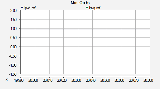
After the real (Ipvd-ref) and reactive (Ipvq-ref) current components in the synchronous reference frame have been computed the quantities Ipvd-ref and Ipvq-ref can be transformed into the three-phase currents in the stationary reference frame (the time domain sinusoidal forms Ipvaref, Ipvbref, and Ipvcref). These current signals are used to control the ideal current source to represent the CSI connected to the grid.
Note that by using the average model, we can ignore the switching of the power switches, and we can assume that it has an infinite switching frequency—i.e., the resulting current is represented by the pure sinusoid generated by the controlled-current source to represent the practical CSI. One major advantage to this is that the simulations can be accomplished in a much shorter time, which allows us to perform many different types of dynamic simulations in power system studies.
CSI—Detail Model
.png)
The hardware of the power converter is represented by the real IGBT in parallel to its flywheel diode. The circuit driver is simulated by the real switching pattern commonly used in an actual power converter. The circuit is connected to the grid, as in the previous section. The only differences are that the ideal current source is replaced by an actual (hardware) power converter with six power switches and the firing control logic is implemented. The fundamental of power electronics converters, applications, and design can be found here [2]
Power-Switching Control
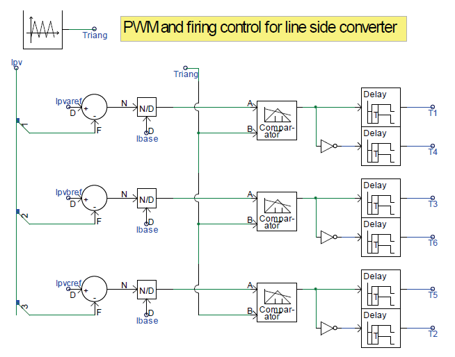
The commanded sinusoidal reference three-phase currents are compared to the actual three-phase currents, and the errors are compared to a triangular waveform with a peak-to-peak value of ±1. The currents are per-unitized by dividing the current errors by the base current. The outputs of the comparators are used as the firing signals to drive the base of the IGBTs; thus, they turn the IGBTs on and off.
The time delays are inserted in series with the firing signals to ensure that the top and bottom pairs of the IGBTs do not turn on at the same time to avoid short-circuiting the DC bus. This time delay is very small, in microseconds (modern IGBTs can turn on and off very fast). The detailed operation of the power converter is well-known technology that can be found in many power electronics textbooks.
Current-Regulated CSI
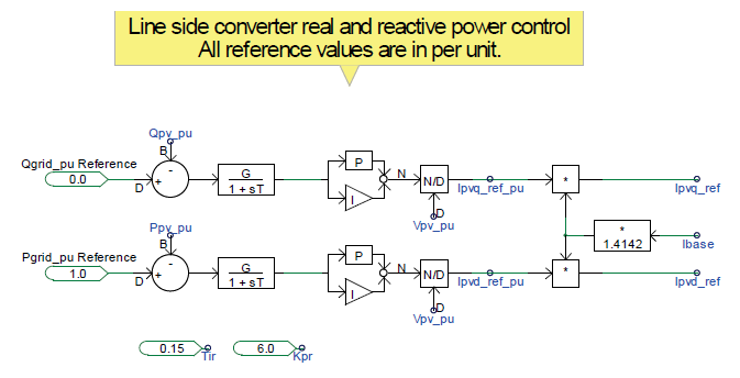
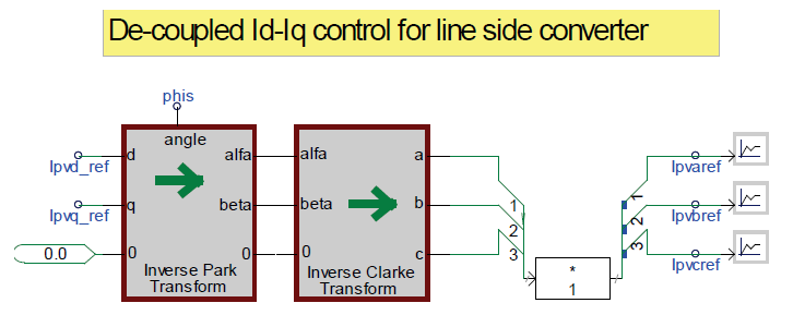


To regulate the real and reactive power output of the power converter, the same technique is used. The real (Id_ref) and reactive current (Iq_ref) components are computed in the synchronous reference frame to obtain the phasor quantities. The rotating reference frame is attached to the phasor voltage, Vpv, and the rotating angle “phis” is found using the phase-locked loop.
The real and reactive current components (Ipvd_ref, Ipvq_ref) in the synchronous reference frame are then transformed back to the three-phase sinusoidal current references (Ipvaref, Ipvbref, Ipvcref) in the stationary reference frame to drive the power switches of the IGBTs.
The per-phase voltage and the line-to-line voltage monitored at the terminal of the power converter are shown on the right. As can be expected, the output of the pulse-width modulation contains a lot of harmonics at the specified switching frequencies (900 Hz).
The line current in Phase A is closer to the sinusoidal current, although the higher harmonic content is still visible. Note that the actual current is synthesized to follow the sinusoidal reference signal, Ipva_ref.
The measured real power and the reactive power at the terminal of the power converter are shown on the right. As the measurements are taken farther from the terminal of the PV inverter, the higher harmonic components of the currents are filtered out and the output voltage and currents look very sinusoidal.
The measurements of the line currents and voltages taken at the high side of the substation transformer are shown on the right. The filtering of the line impedance very effectively cancelled most of the higher harmonics in both the currents and the voltages.
Voltage-Source Inverter (VSI)—Detail Model
.png)


_into_Vpvd_and_Vpvq_in_the_synchronous_reference_frame.png)
_into_Isd_and_Isq_in_the_synchronous_reference_frame.png)


A voltage-source inverter (VSI) synthesizes a voltage source connected to the grid. Because real and reactive power control is generally accomplished by controlling the reference currents, and controlling the voltage does not guarantee a direct response of the output currents, it is common practice to control the current indirectly by controlling the voltage output of the PV inverter. As shown below, the hardware for the VSI and the CSI are identical.
The CR-CSI uses the reference current to generate a current signal to trigger the base drivers of the IGBTs and uses the current feedback to compare and correct the current errors to make accurate syntheses of the PV inverter output current. Thus, the filter inductance (represented by the reactance, Xls) does not have to be included in the equations used to generate the output currents.
The CR-VSI indirectly controls the output current. It uses the voltage feedback Vpv and the corresponding voltage drop across the filter inductance, XlsIs, to synthesize the voltage feedback E that will produce the desired output currents (Is-reference). Thus, the filter inductance, Xls, must be included in the equations used to generate the voltage E.
Consider the phasor diagram of the controller used to generate the voltage E in a CR-VSI. The single-line diagram of the power converter is enclosed in the dashed black lines. First, consider the voltage, Vs, as an input to the phase-locked loop; thus, the d-axis is aligned to the voltage, Vs.
The equations governing the voltage can be written as
\(E=V_{pv}+jX_{ls}I_{s}\)We can decouple the equation into its complex representation as:
\(E_{d}+jE_{q}=\left (V_{pvd}+jV_{pvq} \right )+jX_{ls} \left (I_{d}-jI_{q} \right )\)Or, this can be decoupled into two equations:
\(E_{d}=V_{pv}+X_{ls}I_{q}\) \(E_{q}=V_{pvq}+X_{ls}I_{d}\)The Clarke and Park transformations can be used to transform the terminal voltages (Vpva, Vpvb, Vpvc) in the stationary reference frame into the synchronous reference frame (Vpvd and Vpvq). When the Vpv is used as the input to the phase-locked loop, the d-axis is aligned to the phasor voltage, Vpv, and the phasor, Vpvq = 0, as represented by the phasor diagrams with the reference frame aligned to Vpv.
\(E_{d}=V_{pvd}+X_{ls}I_{q}\) \(V_{pvq}=0\)The q-axis equation can be rewritten as:
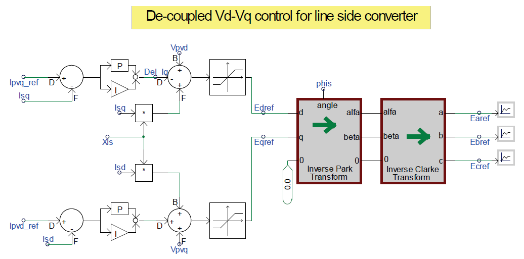
\(E_{q}=X_{ls}I_{d}\)Figure on the right shows the implementation of the voltage reference signals Ed and Eq. Additional input to make any corrections is also implemented using the PI controller to ensure that the reference real power and reactive power can be maintained.
After the voltage reference signals of the Eqref and Edref have been computed in the synchronous reference frame, the three-phase voltage signals (Earef, Ebref, Ecref) in the stationary reference frame can be generated and fed into the firing circuit board of the power converter to turn the IGBTs on and off in the correct sequence.
Figure on the right presents an example of the per-phase voltage and the line-current output of the CR-VSI. Note that the current waveform is less sinusoidal compared to that of the CR-CSI, because the power converter is not commanded to follow the reference currents; instead, it is commanded to synthesize the reference voltages, Earef, Ebref, and Ecref.
Controlling the Grid-Side Inverter and Power Plant

The PV inverter is the point of conversion from DC to AC power. In small residential applications, the PV inverter is usually single phase, converting DC to single-phase AC (60 Hz). The PV array is connected to the PV inverter via a maximum power point tracker to optimize energy conversion from sunlight to electrical power. A PV inverter for large-scale installation usually comes in three-phase arrangements. The PV inverter combines the output of rows of PV strings in DC and converts them to AC. For example, an inverter can processes the output of a PV array with 500 PV modules. Three-phase output rated at 208 V or 480 V is commonly found in commercial PV inverters. Again, it must be emphasized that the topology described here is a single-stage topology, and controls for multi-level and multi-stage converters will require significant modifications from the ones described here.
In this section, we implement a controller based on the controllers developed and recommended by the WECC Renewable Energy Modeling Task Force (REMTF)[3]. A block diagram illustrating an overview of PV power plant control is shown in block diagram representing a PV power plant. From left to right, the highest level of control is implemented first, by the control block REPC; to the REEC, with a focus on the level of the PV inverter; then to the REGC, which is implemented to correct utility interface issues.
- REPC — This supervisory control is implemented to control the real and reactive power of an entire PV power plant. Inputs may include the reference voltage (Vref), reference reactive power (Qref), reference real power (Pref), and reference frequency (Freqref). Thus, the control block functions to control the real power output to respond to a frequency disturbance (and/or governor response) and to respond to a voltage regulation at a bus (at the point of interconnection or at the remote bus).
- REEC — This power-converter control is implemented to limit the currents based on the carrying capability of the power switches (i.e., IGBT and free-wheeling diode). Different types of reactive power control are implemented in this block as well.
- REGC — This generator control is implemented to the grid interface (under-/overvoltage scenarios) and enables nonlinear current control capability.
Device Level
A PV inverter is a mature technology developed early on by the power drive industry for adjustable-speed drives, also known as adjustable-frequency drives, used to control the variable-speed operation of electric machines (e.g., induction motors) with torque or speed-control capabilities. Later, grid-interface technology was also developed extensively by the industry to provide uninterruptible power supply for the computer industry. Thus, the basic operations have been developed based on the experiences gained by the various industries. The details of the design, analysis, and protection at the device level can be found in many power electronics textbooks.
Generator Level
At the generator level, the controller focuses on power-converter control and protection at the power-converter level. Two controllers to serve these functions have been developed by the WECC-REMTF. These controllers are meant to provide good grid integration to allow a PV converter to interface with the utility grid according to local standards and regulations. A PV controller can be set to provide fault ride-through capability, current limit protection, instantaneous and independent control of real and reactive power, and ancillary services to the grid.
REGC
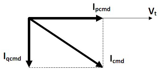
The REGC is the first controller to be implemented and is directly connected to the power converter driver logic. The inputs to this block are the commanded real power (P) current component (Ipcmd) in phase with the voltage (Vt), and the commanded reactive power (Q) current component (Iqcmd), the current component in quadrature (perpendicular) to the voltage Vt. The total current (Icmd) consists of the two components: Ipcmd and Iqcmd. The REGC is intended to ensure that the power converter has ride-through capability when exposed to local disturbances or transmission line faults.
The outputs to this block are the commanded real power (P) current component (Ipord), the current component in phase with the voltage Vt, and the commanded reactive power (Q) current component (Iqord), the current component in quadrature (perpendicular) to the voltage Vt. Both of these quantities (Ipord and Ipord) are the adjusted input values during high- or low-voltage operation.
The REPG uses per-unit quantities and the generator base (PV inverter base; e.g., MBASE = 1.5 MVA) instead of a system base or PV power plant base (e.g., SBASE = 60 MVA). However, if a single-generator representation is used, the REPG uses MBASE = SBASE.
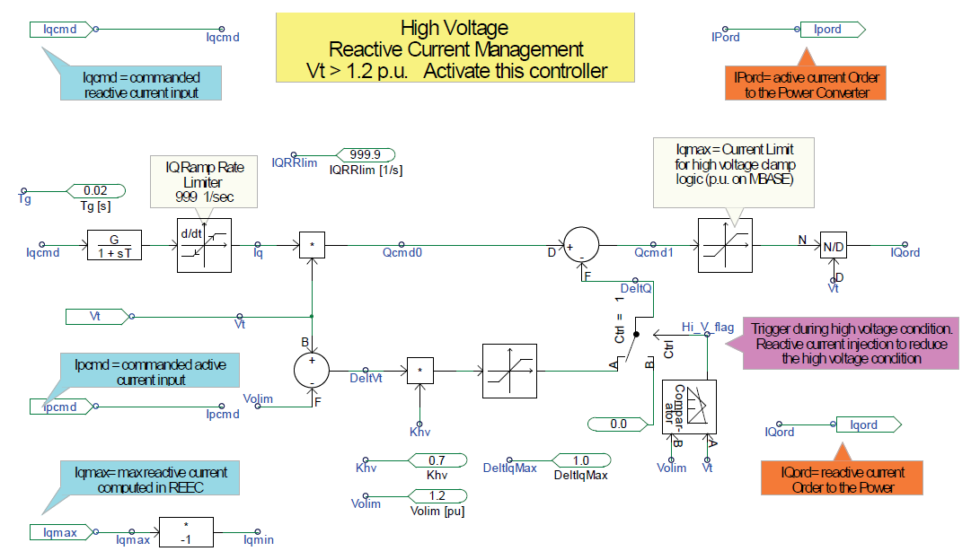
As shown in the Block diagram illustrating the HVRCM controller to inject additional inductive current during a high-voltage event, the high-voltage reactive-current management (HVRCM) functions to alter the control behavior of the reactive power during high-voltage operation (e.g., higher than 1.2 p.u.), and the low-voltage active-current management (LVACM) functions to alter the control behavior of the active power during low-voltage operation (e.g., lower than 0.9 p.u.).
High-Voltage Region
The block diagram shown on the right can be used to describe the control functions of the HVRCM. The term reactive current is used to describe both the inductive current and capacitive current. Inductive current is the current that causes a power converter to absorb reactive power, and the capacitive current is the current that causes a power converter to produce reactive power.
The HVRCM has the control property to change the output reactive current command (Iqcmd) by providing an additional inductive current injection to decrease the reactive power output of the power converter, thus indirectly reducing the terminal voltage of the power converter. It also has a ramp-rate limiter to limit the rate of change in the reactive current output.
In analogy to the droop, in a power plant governor this HVRCM also functions to increase the inductive current to draw more reactive current from the grid, thus, in effect, reducing the terminal voltage.
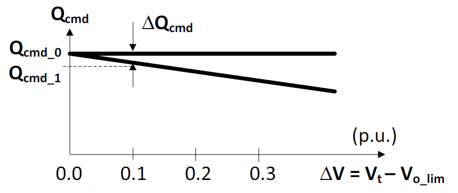
Figure on the right describes the changes in reactive power command if the terminal voltage (Vt) exceeds the threshold voltage (Volim). The slope of the line is specified as the constant (Khv).
Note that the additional current injection is not activated until the level of the terminal voltage passes the overvoltage limit (Volim). The sensor used to activate this function is embedded in the comparator with the logic output Hi_V_flag = 1.
Under normal circumstances (the logic output Hi_V_flag = 0)
\(\Delta Q=0\) \(I_{qcmd1}=I_{qcmd0}\)However, when the Hi_V_flag = 1, the inductive current injection is activated, and the following equations are used to govern the output of the inductive current injector:
\(\Delta V_{t}=V_{olim}−V_{t}\) \(\Delta Q=Q_{cmd0}−Q_{cmd1}\) \(\Delta Q=K_{hv}· \Delta V\) \(I_{qcmd1}=I_{qcmd0}−\frac{\Delta Q}{V_{t}}\)Take, for example, Volim= 1.2 p.u., Khv = 0.7, the initial Iqcmd = 0.1 p.u. at the terminal voltage of Vt = 1.0 p.u. The terminal voltage suddenly increases to Vt = 1.3 p.u. because of an external disturbance. The reactive power, which was initially Qcmd_0 = 0.1 p.u. during the high-voltage event, decreases to Qcmd_1 = (0.1 – 0.07) p.u. = 0.03 p.u.Note that the current limiter is placed to ensure that the Iqmax (computed in the REEC block) is not exceeded.
The choice of Khv is certainly determined by the local power system network. If the voltage in the local network varies a wide range above normal, the value of Khv can be adjusted accordingly. The impact from a single PV inverter to suddenly change the voltage level may not be significant; however, the collective impact of hundreds of PV inverters connected to the grid following the same command will definitely be very effective. Also note that the current limits must be set to the limit of the reactive power capability of the power converter. These currents are limited before the commanded currents are passed to the power switches via the variable Iqord.
Low-Voltage Region
_during_a_low-voltage_event.png)
The block diagram illustrating the LVACM controller to adjust the real current component during a low-voltage event can be used to describe the control functions of the LVACM. The term active current is used to describe the real or active power component (e.g., Ipcmd or Ipord).
In summary, the LVACM allows two choices determined by the low-voltage power logic, or LVPL (the upper limit of Ipcmd), switch. If LVPL = 1, the upper limit of the real power current component Ipcmd is governed by the nonlinear map LVPL compared to Vt. If LVPL = 0, the upper limit of the real power current component Ipcmd is governed by Ipmax computed in another controller block called REEC.
The Block diagram illustrating the LVACM controller to adjust the real current component during a low-voltage event shows two quantities that should be computed. The first one is the scaled voltage (Vt_scaled), and the second one is the upper limit of the real current component (LVPL).
Computing Vt_scaled

Consider the Vt_scaled computation. Vt_scaled is computed from preprogrammed map shown in scaled voltage to adjust the Pord during a low-voltage event. During a low-voltage event, the commanded power (Pord) must be scaled down to accommodate the current-carrying capability of the power switches (IGBT and diodes). The Pordshould be scaled such that the resulting Ipord current will be within the allowable limit.
For example, if the original commanded power Pord = 1.0 p.u., under normal voltage (Vt = 1.0 p.u.), the commanded real power stays the same. Suppose during a grid disturbance the voltage drops to Vt = 0.6 p.u.; without scaling, the computed current command would be very high (Ipcmd = Pord/Vt = 1.0/0.6 = 1.67 p.u.), which is much larger that the allowable current limit (Ipmax ~ 1.2 p.u.). Thus, by scaling the voltage accordingly, the new Pord= Vt_scaled x 1.0 p.u. = 0.4 x 1.0, which gives the new Pord = 0.4 p.u.
Note that when voltage is within the normal range (0.9 p.u.< Vt < 1.1 p.u.), the power converter must be capable of delivering Pord = 1.0 p.u.; thus, the voltage is scaled to 1.0 for voltages Vt > 0.9 p.u. For example, at Vt = 0.9 p.u., the Pord = 1.0 p.u. and Ipcmd = 1.11 p.u., which is within the maximum current limit.
Computing LVPL
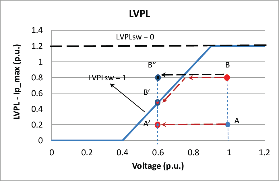
The second quantity of interest is the LVPL. This quantity is actually the upper limit of the real power component. There are two options based on the position of the logical switch, LVPLsw. If LVPLsw = 0, the value of LVPL is set to Ipmax (computed in the REEC block and indicated by the thick, bold, black line shown in LVPL calculation to set the upper limit of Ipcmd during a low-voltage event); on the other hand, if LVPLsw = 1, the value of LVPL is computed by using the nonlinear map shown above.
Unlike using the map for the scaled voltage presented previously, using the LVPL map may or may not affect the outcome of the commanded output power Pord; instead, this map is applicable only to the commanded current output, Ipcmd. For example, under normal voltage (Vt = 1.0 p.u), Ipcmd = 0.2 p.u. If the voltage suddenly drops to 0.6 p.u., indicated by Point A on the map, the computed LVPL = 0.48 p.u.; thus, it does not affect the Ipcmd (i.e., at Vt = 0.6 p.u.) the Ipcmd is not limited, and it is the same as the original value (Ipcmd = 0.2 p.u., indicated by Point A’). On the other hand, if the original Ipcmd = 0.8 p.u. (at Vt = 1.0 p.u., as indicated by Point B) and the voltage suddenly drops to Vt = 0.6 p.u., the commanded Ipcmd must be limited to Ip_LVPL = 0.48 p.u., as indicated by Point B’ in the map. Note that within the normal voltage range, the current is limited to Ipmax. (Ipmax is set to 1.2 p.u. in this particular map for 0.9 p.u. < Vt < 1.1 p.u.)
If LVPLsw = 0, the value of LVPL is set to Ipmax. If the original Ipcmd = 0.8 p.u. (at Vt = 1.0 p.u., as indicated by Point B) and the voltage suddenly drops to Vt = 0.6 p.u.; the commanded Ipcmd will stay the same as the upper limit of the Ip_LVPL = 1.2 p.u. Thus, the operating point will move from Point B at Vt = 1.0 p.u. to the new operating point at Vt = 0.6 p.u., then to a new operating point as indicated by Point B” in the map.
Revised Commanded Power Pord in the Low-Voltage Region
The revised commanded power Pord, computed based on the output of the Vt scaler and LVPL, can be different for different power levels and different settings of the LVPLsw logic switch.
- Example 1
Normal condition Pord_orig = 0.8 p.u.; Vt = 1.0 p.u.; and Ipcmd = 0.8 p.u.
LVPLsw = 1. The voltage drops to Vt = 0.6 p.u., Pord_new = Vt_scaled x Ipcmd_limited = 0.4 x 0.48 = 0.192 p.u., and the new Ipcmd = Ipord = 0.192/0.6 = 0.32 p.u.
LVPLsw = 0. The voltage drops to Vt = 0.6 p.u., Pord_new = Vt_scaled x Ipcmd_limited = 0.4 x 0.8 = 0.32 p.u., and the new Ipcmd = Ipord = 0.32/0.6 = 0.533 p.u.
- Example 2
Normal condition Pord_orig = 0.2 p.u.; Vt = 1.0 p.u.; and Ipcmd = 0.2 p.u.
LVPLsw = 1. The voltage drops to Vt = 0.6 p.u., Pord_new = Vt_scaled x Ipcmd_limited = 0.4 x 0.2 = 0.08 p.u., and the new Ipcmd = Ipord = 0.08/0.6 = 0.133 p.u.
LVPLsw = 0. The voltage drops to Vt = 0.6 p.u., Pord_new = Vt_scaled x Ipcmd_limited = 0.4 x 0.2 = 0.08 p.u., and the new Ipcmd = Ipord = 0.08/0.6 = 0.133 p.u.
Thus, the impact of the controller on the outcome of the commanded active power component is significant for medium to rated power when the LVPLsw is activated. However, when the active power command is low, it makes no difference whether the LVPLsw is activated or not.
REEC
The REEC is designed to control the real and reactive power (under normal and transient conditions). The REECuses per-unit quantities and the generator base (PV inverter base; e.g., MBASE = 1.5 MVA) instead of a system base or PV power plant base (e.g., SBASE = 60 MVA). However, if a single-generator representation is used, the REPG uses MBASE = SBASE.
Control Implementation of Reactive Power and Voltage Control

The block diagram illustrating the computation of the reactive power input command Qin illustrates the control mechanism of the reactive power control. Two stages are considered. This controller controls the reactive power to match the reactive power command, Qin. The Qin is the input to the PI controller to regulate the reactive power or voltage, as shown in reactive power and voltage control diagram (enclosed in the solid black line). For now, ignore the blocks NoFreeze and Freeze and assume that these blocks are shorted.
Logical Switch PF_flag
If the controller is set to control the reactive power output of the power converter (Vflag = 1; see the description of Vflag below), two options are available to control the reactive power output.
- PF_flag = 1 sets the reactive power input command to follow Qpf computed based on a constant power factor pfaref. The reactive power is commanded to be proportional to the actual real power Pe output; thus, it varies with the actual output power Pe as the output changes, except when the pfref = 1; however, in this case, the reactive power is commanded to be zero at all times. The Qpf calculation can be shown as:
- PF_flag = 0 sets the reactive power input command to follow the external reactive power command Qext. This input can be driven by supervisory control within the supervisory control domain (i.e., the REPC block diagram).
Logical Switch Vflag

The logical switch Vflag functions to control the reactive power output of the power converter. This block is inside the rectangle marked by the dashed red line. The input to this block is the output of the first block, and it may take two branches or directions, depending on the Vflag set. Focus on the circuit enclosed in the rectangle marked by the thin red line.
- Vflag = 1. The logical switch is set to A, then the reactive power control is chosen. The reactive power output will be controlled to match the reference Qin.
- Vflag = 0. The logical switch is set to B, then the voltage control is chosen. Note that the limiter placed before the Vstar will limit the value of Vstar (thus, the Vref1) within the acceptable voltage level (Vmin < Vstar < Vmax). The terminal voltage Vt will be controlled to match the reference voltage Vref1.
Logical Switch Qflag
The output from the block enclosed in the red rectangle shown in the reactive power and voltage control diagram will be the input A to the next logical switch (shown in the light blue ellipse) and to the next stage to calculate the commanded reactive current Iqcmd. The logical switch is activated by the Qflag. The logical switch Qflag functions to determine if the reactive power output will be controlled via the two PI controllers (within the rectangles marked by the solid black line and the solid red line) or via the linear path (within the rectangle marked by the black dashes and dots).
- Qflag = 1 and Vflag = 1. The reactive power is accomplished via the PI controller inside the rectangle marked by the solid black line and the PI controller inside the rectangle marked by the dashed red line (two PI controllers in series).
- Qflag = 1 and Vflag = 0. The voltage is controlled by the PI controller shown inside the rectangle marked by the dashed red line (a single PI controller).
- Qflag = 0. The reactive power is controlled by a feed-forward linear loop without the PI controller (see the rectangle marked by the black dashes and dots). This loop will allow the reactive power to be controlled externally—for example, by supervisory control via the variable Qext to accomplish plant-level reactive control by paralleling the response of all the PV inverters within the PV plant (see the REPC block diagram).
Identifying Abnormal Voltage Range

Another logical switch is the one encircled within the dashed green ellipse shown in the reactive power and voltage control diagram. This logical switch enables the injection of additional reactive current, Iqinj, during abnormal voltage (either in the overvoltage condition when the voltage Vt > Vup or in the undervoltage condition when the voltage Vt < Vdip.
Figure on the right shows the logical switch Volt_dip. This logical switch will be operated based on the detection of the terminal voltage, Vt, as shown in the diagram.
- Volt_dip = 0 is a normal condition, and the injection current Iqinj = 0.
- Volt_dip = 1 is an abnormal condition, and the injection current is used based on the droop characteristic.
The output commanded reactive current, Iqcmd, is limited by its maximum, Iqmax, and its minimum, Iqmin. Calculating Iqmax and Iqmin will be shown in a later section.
Additional Reactive Current Injection, Iqinj
.png)
.png)
The additional reactive current injection is computed based on the size of the voltage deviation of the terminal voltage, Vt, from the reference voltage, Vref0.
Calculating an additional reactive current injection is done with the linear model shown in the diagram illustrating an additional reactive current injection during an abnormal voltage event (Volt_dip = 1). This controller block includes the deadband db1 and db2 to disable the control from injecting the additional reactive current, Iqinj, when the voltage is within the normal range. In most cases, the reference voltage is assumed to be Vref0 = 1.0 p.u., and the normal voltage range 0.9 p.u. < Vt < 1.1 p.u.; thus, the deadbands db1 = db2 = 0.1 p.u. The constant value Kqv is the slope affecting the aggressiveness of the current injection, Iqinj, to correct the voltage deviation. Note that the impact of the controller is dependent upon the stiffness of the grid, the availability of current-carrying capability of the power converter to pass this additional current, and the control setting of the PQflag. However, db1, db2, Kqv, and Vref0 can be adapted to the new values to follow specific regional and/or local rules and regulations.
Block diagram illustrating a method to compute an additional reactive current injection during an abnormal voltage event (Volt_dip = 1) shows the control block diagram implementation of the additional current injection based on the voltage condition.
Real Power Control

Because the relationship of the reactive power to the terminal voltage is very tight, either the reactive power control or the voltage control is generally chosen. The reference real current component, Ipcmd, can be computed by dividing the reference power, Pref, by the terminal voltage.
The block diagram illustrating a method to compute the real current component, Ipcmd illustrates the following calculation:
The current limiter is used to limit the Ipcmd to the allowable Ipmax based on the setting of the PQflag (P-priority or Q-priority).
Calculating the Maximum and Minimum Current of Ipcmd and Iqcmd


To prevent the power switches (IGBTs and diodes) from conducting current higher than the current-carrying capability, the control block diagram illustrating a method to compute the current limits for the real and reactive current components can be used to implement overcurrent protection.
Two type of priorities can be set through the PQflag.
- PQflag = 1 is also known as P-priority. The controller’s priority is to maximize the range of the real current component, Ipmax, and use the remaining current capability for the reactive current component, Iqcmd.
- PQflag = 0 is also known as Q-priority. The controller’s priority is to maximize the range of the reactive current component, Iqmax, and use the remaining current capability for the real current component, ”’Ipcmd.
Figure on the right illustrates the operation in P-priority and Q-priority. During a normal condition, the terminal voltage is assumed to be Vt = 1.0 p.u., and the maximum current allowed is Imax = 1.3 p.u. We assume initially that the output real power P = 0.8 p.u. Ipcmd = 0.8 p.u., and the reactive power Q = 0.2 p.u., Iqcmd = 0.2 p.u.; thus, the initial current is shown as the phasor I1.
The operation of P-Priority and Q-Priority is triggered by the logic diagram shown inside the red ellipse. Unless stated differently for different projects, during normal operation the P-Priority is set to maximize the energy yield of the renewable energy resources; thus, P-Priority is enabled (PQflag = 1) during normal operation (when the logic Volt_dip = 0). Even during abnormal voltage (V_dip = 1), the P-Priority can be activated (PQflag = 1) under certain circumstances.
Operation in P-priority
The left part of the phasor diagram illustrating the P-priority and Q-priority illustrates the operation when P-priority option is selected. When a disturbance in the transmission line occurs, the voltage drops to Vt = 0.5 p.u. Using the P-priority, we can compute the maximum
\(I_{pmax}= \sqrt{1.3^2 – 0.2^2} = 1.28\)p.u. Because the operation is set to P-priority, the controller tries to maintain output power constant at P = 0.8 p.u.; however, this requires
\(I_{pcmd} = \frac{0.8}{0.5} = 1.6\)p.u., which is higher than the allowable Ipmax = 1.28 p.u. Thus, we have to settle to Ipcmd = 1.28 p.u., and Iqcmd = 0.2 p.u. is frozen and must stay the same as the value before the voltage drop, and the output current changes from I1 to I2.
Operation in Q-priority
The right part of the phasor diagram illustrating the P-priority and Q-priority illustrates the operation when the Q-priority option is selected. When a disturbance in the transmission line occurs, the voltage drops to Vt = 0.5 p.u. Using the Q-priority, we can compute the maximum
\(I_{qmax} = \sqrt{1.3^2– 0.8^2} = 1.02\)p.u. Because the operation is set to Q-priority, the controller tries to maintain the output reactive power constant at Q = 0.2 p.u. Thus, the required
\(I_{qcmd} = \frac{0.2}{0.5} = 0.4\)p.u. This value is the maximum range of allowable Iqmax = 1.02 p.u. The phasor current I1 moves to I3. Note that the magnitude of the phasor I3 = 0.89 p.u., which is less than the maximum current limit Imax = 1.3 p.u.
Next, consider the additional current injection, Iqinj, to support the voltage during the voltage dips. In this case, assume that Kqv = 2.0 and Vref0 = 1.0 p.u. When the voltage, Vt, drops to Vt = 0.5 p.u. The additional injection current is
p.u.; thus, including the current injection, Iqinj, the total
\(I_{qcmd} = 0.4 + 1.0 = 1.4\)p.u. However, the Iqmax = 1.02 p.u. In this case, we have to settle with Iqcmd = 1.02 p.u. and Ipcmd = 0.8, and the total current
\(I_{4}= \sqrt{1.02^2 – 0.8^2} = 1.3\)p.u.
Controlling the Freeze During Abnormal Voltage Conditions

It is common in a PV inverter to freeze the states that control the output of the reactive power. This is done during the transients, so that the impact of the short disturbance does not exaggerate the situation and make the power system unstable when the disturbance is removed the grid. In some applications, the output current is frozen until the disturbance is over; however, this will only limit the output current contribution to the fault. The implementation is shown in block diagram illustrating a method to freeze the operating current during voltage dips.
Plant Level

A PV plant consists of many large inverters connected in parallel by miles of AC cables (also known as a collector system). Supervisory control is implemented to the inverters within the power plant to achieve plant-level objectives. As the level of PV penetration increases, PV plants are required to provide low-voltage and high-voltage ride-through capabilities and different types of ancillary services (reactive power support, oscillation damping, inertial response, governor control, spinning reserve, etc.) to the power system network. In large power system studies (such as WECC-wide studies), it is common to represent a wind power plant or PV plant as a single generator, as shown in single-line diagram illustrating a PV plant with a single generator.
As shown, the output of a PV inverter is usually 208 V or 480 V. In the example presented above, the output voltage of the 165-kVA, three-phase PV inverter is 480 V; this is a parallel combination of many inverters representing a PV plant.
The transformers (480 V/34.5 kV) are connected to a substation transformer. Several of these nodes are connected in a daisy-chain fashion, which is then connected to the substation transformer (66 MVA, three-phase, 34.5 kV/110 kV). It is customary for the utility meters to be connected at the high side of the substation transformer to measure the revenue of a PV plant.
REPC
The REPC module shown in control block diagram illustrating voltage regulation for a remote bus is a very useful way to implement the ancillary service capabilities of a renewable energy generator as required by the system operator. The REPC control block can be used to implement supervisory control to both the real and reactive power. Note the capability of the power converter to deliver the desired output and that the current-carrying capability of the power switches (IGBTs) takes precedence over the objective function specified in the REPC. For example, if the current/voltage limit of the IGBT has been reached, and the REPC objective function has not been accomplished, the final outcome will be determined by the IGBTs current/voltage limit.
Like REPG and REEC, the REPC uses per-unit quantities; however, in the REPC, the base quantity used is the system base (a PV power plant base) instead of the generator base (a PV inverter base).
Voltage Control at a Remote Bus


As shown in single-line diagram illustrating a method to accomplish different remote voltage regulations, the remote bus is defined as the bus farther from the terminal voltage. The electrical distance from the terminal voltage is represented by the reactance Xbr, the current flowing through the branch is represented by Ibranch, and the reactive power flowing in the branch is represented by Qbranch.
The regulated voltage is located in a remote bus from a monitored bus voltage Vreg. Two types of voltage compensation can be activated in the REPC block diagram:
- VcompFlag = 1 — The voltage to be controlled is measured from the Vreg, bus and it is compensated by using the computed voltage drop I X.
Example 1 — If you want to regulate V1 (high side of the transformer) and have access only to the voltage Vt, then to control V1, the branch current Ibranch = Ixfrmr and Xbr = Xxfrmr; voltage Vreg = Vt; and the voltage drop is computed from Ixfmr Xxfmr.
Example 2 — If you want to regulate V2 and monitor only the voltage V1, then to control V2, the branch current Ibranch = Ibranch1 and Xbr = Xs; the voltage Vreg = V1; and voltage drop is computed from Ibranch1 Xs.
- VcompFlag = 0 — The voltage to be controlled is measured from the Vreg bus, and it is compensated by estimating the voltage drop by Kc Qbranch.
Example 1 — If you want to regulate V3 and have access only to the voltage V2, then to control V3, the Qbranch = Qbranch1 and voltage Vreg = V2, and the voltage drop is estimated by Kc1 Qbranch1.
Example 2 — If you want to regulate V1 and you have access only to the voltage Vt, then to control V1, the Qbranch = Qout and voltage Vreg = Vt, and the voltage drop is estimated by Kcxfmr Qout.
Reactive Power Control
The reactive power control is illustrated by the control block diagram illustrating a method to regulate reactive power. In this control block diagram, there is a logical switch called RefFlag that must be set to make the following choices:
- RefFlag = 1 — Configure the controller to regulate the voltage based on the measured voltage ‘Vreg.
- RefFlag = 0 — Configure the controller to regulate the reactive power flow in a specified branch (for example, the Qbranch1 in Branch 1 or Qout measured at the output of bus Vt) to follow the reference, Qref. Caution must be taken when controlling a branch from a PV power plant when the output is split into multiple branches. For example, we can control the reactive power flow in a particular branch to follow a certain reference Qbranch = Qbranch1; however, the setup will let us control the reactive power flow only in a single branch, so if we control only the reactive power flow in Branch 1, we do not have any control over the power flow in Branch 2. Because the output of the power plant flows in both Branch 1 and Branch 2, the power plant may have reached its upper limit before Qbranch1 = Qref is reached.
The output of this controller is the Qext, which is an input to the next block, REEC, and will be used to compute the reactive current component, Iqcmd, that will generate the requested Qext. Note that Qext is either the reference reactive power Qref (for RefFlag = 0) or the equivalent reactive power needed to regulate the voltage at a specified remote bus (for RefFlag = 1).
Real Power Control
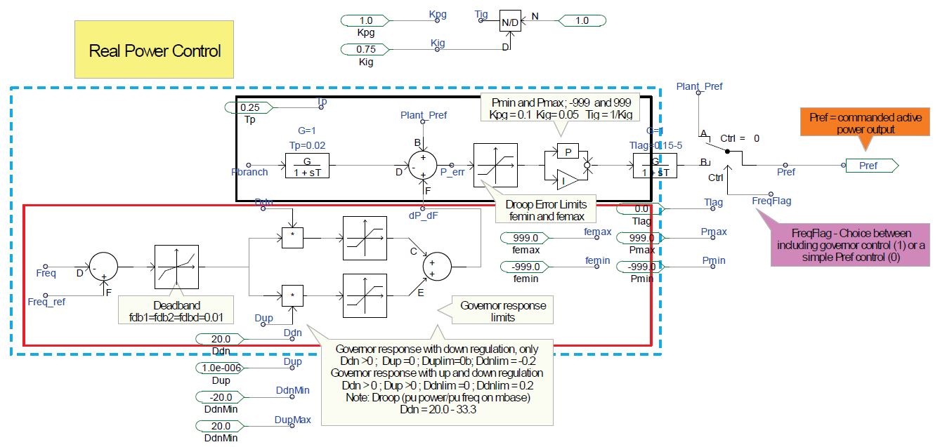

The real power control is illustrated by the control block diagram shown in figure on the right. The reference power is set by the reference power Plant_Pref. The diagram shown in single line diagram describing real power control in remote location is an example of how to use reference power Plant_Pref. For example, if the output power of a PV power plant is to be controlled to follow the reference Plant_Pref, then we can set Pbranch = Pout.
Caution must be taken when controlling a branch power flow from PV power plant when the output is split into multiple branches. For example, we can control the power flow in a particular branch to follow Plant_Pref by setting Pbranch = Pbranch23 or Pbranch = Pbranch1. However, the setup will let us control the power flow only in a single branch; thus, if we control only the power flow in Branch 1, we do not have any control over the power flow in Branch 2. The power plant may have reached its upper limit before Pbranch1 = Plant_Pref is reached.
This control block diagram shows a logical switch called FreqFlag that must be set to make the following choices:
- FregFlag = 1 — Configure the controller to regulate the real power flowing in the specified branch Pbranch using the PI controller to include the reference Plant_Pref and the frequency response
\(\frac{dP}{dF}\). At this point, the only way to disable the frequency response\(\frac{dP}{dF}\)into the power command mix is to set the slope Ddn = Dup = 0. - FreqFlag = 0 — Configure the controller to regulate the reactive power flow in a specified branch Pbranch to follow the reference real power command Plant_Pref using the feed-forward linear path (bypassing the PI controller) without the influence of frequency response.
The output of this controller is the Pref, which will be used as an input to the next block, REEC, and to compute the real current component Ipcmd that will generate the requested Plant_Pref.
The real power control following the path with the PI loop lies within rectangle marked by the blue dashes. The diagram within the red rectangle is the frequency response control, and the diagram within the black rectangle is the total control of real power to match the real power flow within the branch to match the reference Plant_Pref.
Additional Real Power Boost to Respond to Frequency Changes

The additional real power control to support frequency regulation is illustrated by the control block diagram shown within the red rectangle in control block diagram illustrating a method to regulate real power. The reference frequency is set by Freq_ref. The measured frequency is the Freq. The error ΔFreq is passed through the deadband block, and the slope is controllable via the parameters Ddn and Dup, and the output is limited by the limiter DdnMin and DupMax. Graphical illustration of real power regulation during a frequency excursion shows a graphical illustration of this concept. Note that the characteristics can be made nonsymmetrical to perform governor control and frequency response.
PV Dynamic Model Validation

Dynamic model validation is not an easy task to perform and includes many stages. Ideally, as much information as possible is needed. In a dynamic simulation, enough information may not be available to simulate an actual PV plant that we want to validate. In such a case, assumptions about the missing data have to be made; however, in some cases, the validation simply cannot be performed. On the other hand, having too much but inaccurate information may lead to a bad validation and an inaccurate representation of a PV inverter or PV plant.
A typical model validation will represent a PV plant as shown in single-line diagram illustrating the dynamic model validation, in which a single PV inverter represents the total generation of an entire plant. The first step-up transformer connecting the PV inverter to the collector system is used to step up the voltage from low voltage to medium voltage (e.g., 480 V/34.5 kV). The collector system represents the lines or cables interconnecting the step-up transformer within the power plant to the substation transformer, where all the output of the PV inverters within the PV plant are stepped up to the transmission-level voltage (e.g., 34.5 kV/230 kV) to be transmitted over long distances. This collector system can be aggregated into a single impedance represented by Zcollector.
The recorded voltage measured at the point of interconnection is used to drive the simulation as the infinite voltage source at the point of interconnection. The simulation output of the real and reactive power as well as the output currents were compared to the measured data.
Three-Phase PV Plant Validation
Detailed Model Implementation


_voltages_measured,_(b)_currents_measured,_and_(c)_currents_simulated.png)
A detailed model of the circuit implementation is shown in figure on the right. To prepare for dynamic validation, the data measured at the point of interconnection is used as the input to the detailed model; these are usually three-phase voltages and currents. The real and reactive power output can be computed, or it can be obtained from the data recorder. Note that the real and reactive power from the calculation may contain high-frequency noise, whereas the output data obtained from the measurement is usually filtered. For the purpose of the validation, we use a moving average filter for the real and reactive power output computed from the measured three-phase voltages and currents.
The initial condition (pre-fault) of the simulation is adjusted to match the pre-fault measured data. The measured values of the real and reactive power as shown in figure on the right are used to adjust the commanded real and reactive power. The measured data is shown in blue, and the simulated results are shown in green. As shown, the simulation very closely follows the actual output measurement.
In a real set-up, ideally the solar irradiance should be the input; however, this information is seldom available, and—in addition to the transient model analysis, in which the duration of the observation is only a few seconds—this input is less important; thus, we assume that the solar irradiance is constant during the disturbance. The real and reactive power in the pre-fault condition is used to set the real and reactive power commands (reference real and reactive power). These reference values are considered to be constant for the duration of the fault. During the fault the result of the simulation indicates that the real and reactive power changes. That is a result of the control actions of the PV inverter, and it is not because of the reference values of the real and reactive power that are changing during the disturbance. A comparison of the reference values to the measured values shows that the controller of the dynamic models functions properly.
The voltage applied to drive the simulation is shown in the top row of the voltage and current waveforms using a detailed model representation. The PV plant responded to this voltage, thus generating the current waveforms shown in the bottom row of the voltage and current waveforms using a detailed model representation. A comparison of the measured current waveforms to the simulated waveforms indicates that the dynamic model and the controller represent the actual PV plant. Note that the output current, real power, and reactive power are determined by the voltage and the control parameter set for this particular PV plant or PV inverter. By comparing the output real and reactive power shown in figure on the right to the output currents shown in the voltage and current waveforms using a detailed model representation (simulated versus measurement), we can conclude that the PV plant dynamic model very closely represents the actual plant.
Average Model Implementation

The average model of the circuit implementation is shown in figure on the right. The process to prepare for dynamic validation of the average model is the same as that described in the detailed model representation.
The upper part of the comparison of the simulation output to the measured output for an average model shows the real power compared to the reactive power, and the lower part shows the voltage and current waveforms measured at the point of interconnection. This is the voltage used to drive the simulation. A comparison of simulation results shows that there is almost no difference between the detailed model and the average model. Also, a comparison of currents shows that the current waveforms from the detailed model are very similar to the current waveforms from the average model. The only difference is the apparent harmonics shown in the output of the detailed model, but the fundamental components are very closely matched.
Single-Phase PV Plant Validation


In this section, a single-phase PV plant is validated against the measured data. This small-scale PV plant is illustrated in the circuit diagram presented in figure on the right.
The voltage used to drive the simulation and the corresponding real and reactive power output shows the voltage waveforms measured at the point of interconnection. This is the voltage used to drive the simulation. The voltage dip is caused by a fault occurring in the transmission far away from the PV plant.
The real and reactive power output shown on the right in the voltage used to drive the simulation and the corresponding real and reactive power output are the output of the simulation and the measured output. As mentioned previously, the measured data of the real power and the reactive power are filtered and the simulated output of the real and reactive power shows 120-Hz ripples, which is a typical characteristic of single-phase output power.
The output currents are shown in figure on the right.
References
- ↑ NREL, User Guide for PV Dynamic Model Simulation Written on PSCAD Platform, November 2014, [Online]. Available: http://www.nrel.gov/docs/fy15osti/62053.pdf. [Accessed July 2015].
- ↑ Mohan, N.; Undeland, T.M.; Robbins, W.P. Power Electronics: Converters, Applications, and Design. 3rd edition. ISBN-13: 978-0471226932, ISBN-10: 0471226939. New York: Wiley, October 10, 2002.
- ↑ WECC-REMTF. Generic Solar Photovoltaic System Dynamic Simulation Model Specification. Salt Lake City, UT: September 2012.
